META ROSETTA
Mid-Infrared dielectric metasurface
This is a Paragraph. Click on "Edit Text" or double click on the text box to start editing the content and make sure to add any relevant details or information that you want to share with your visitors.

Mid-Infrared Metalens
Our company has designed the mid-infrared metalens that operates in the mid-infrared with a wavelength of 8-14 µm, using easily obtainable silicon wafer and mature semiconductor process technology to replace the traditional silicon germanium lenses of infrared camera.

SEM Image of Mid-Infrared Metalens
The mid-infrared metalens we designed is a product with a propagation phase cycle and a donut-shaped structure. It is manufactured using a 248 scanner of KRF process, and the material is a silicon wafer. Due to the mature manufacturing process and easy acquisition of materials, it has the advantages of lower cost and mass production.
MTF Chart

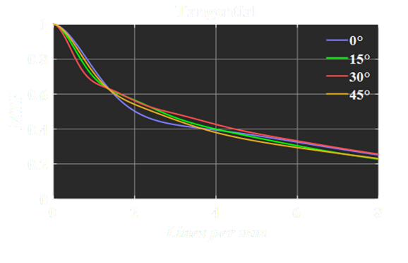
From the MTF graph, we can see the resolution of the metalens under different fringe densities. The graph shows that the MTF curves of different incident angles are almost overlapping from 0 degree to 45 degree, showing that the edge sharpness of the metalens image is almost the same as that of the center.
Advantages of Mid-Infrared Metalens
Lightweight and Compact Design
Multifunctional Integration
Compared to traditional curved lenses, metalenses are thinner and lighter, significantly reducing the size and weight of optical systems.
Capable of incorporating multiple functions, such as adjustable focal lengths, multi-band imaging, or polarization control, into a single optical component, simplifying system complexity.
Manufacturing Flexibility
Various Applications
Compatible with modern semiconductor fabrication processes (e.g., electron beam lithography or nanoimprint lithography), enabling mass production of high-precision components with consistency.
MIR metalenses are valuable in fields such as defense and security (e.g., thermal imaging), medical diagnostics (e.g., spectroscopic analysis), industrial inspection (e.g., gas sensing), and astronomical research.